It took me a while to figure out what I was looking at.
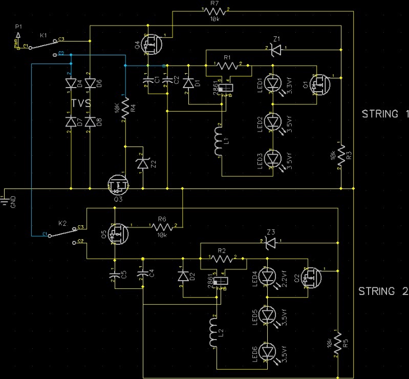
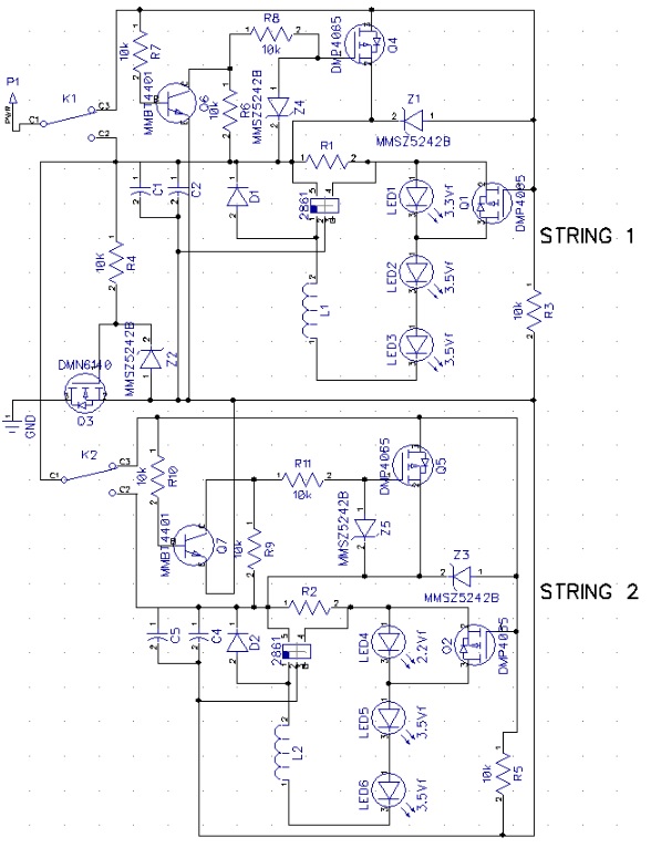
Talking for now only about string 1, the core of the circuit is C1, C2, D1, R1, L1, LEDs 1-3 and the 2861 (which it took me a while to figure out was a PAM2861 LED driver chip). This core is a constant current LED driver circuit using buck-mode switching topology that allows high efficiency with large difference between input and output voltages.
D4, D6-8 are transient suppression, and Q3, Z2, and R4 are reverse polarity protection. The other components appear to be there to turn LED1 on and off without changing LED2 and LED3.
Let's look at these step by step.
The basic driver circuit looks fine. As you haven't put values in, I can't say whether you've made good choices. Maybe you haven't made any yet. I'll assume you can pick proper values there.
Unless K1 and K2 are wired at some distance from the rest of the circuit, I would wire the anode of D4 to P1 and eliminate D6 and D8. D4 and D7 could be combined in a single bidirectional TVS.
Most power mosfets can handle +/- 20V on the gate, so with a 12V supply, Z2 is probably unnecessary, especially if your transient suppression is good. That said, it's not doing any harm, so you may want to leave it in.
Now about switching LED1 on and off. Turning on Q1 would short LED1, thus effectively turning it off. The driver will compensate for the lower voltage drop in the string. This part of the design seems over-engineered to me. Since K1 cannot be used for anything other than turning LED1 on and off, why not just put K1 across LED1 and be done?
The circuit as originally designed (not as shown here) could be useful if K1 were in fact a 3-position switch with an off position. You could then use the single switch to allow 3 states: off; all on; LED2 and LED3 on.
As drawn here, Q4 cannot be turned on. In order to turn on an N-channel FET, the gate needs to be driven positive with respect to the source. This can't happen because the gate is tied to the lowest voltage in the circuit (ignoring drop across Q3, which should be very small).
A P-channel FET is turned on by driving the gate negative WRT the source. I'm guessing in the original design Q4 was a schottky diode and Q1 was a Pfet. In this case, when the circuit is powered through C2, the diode would be reverse biased and R3 would pull the gate of Q1 low, turning it on and shorting LED1. If the circuit were powered through C3, the diode would be forward biased and the gate of Q1 would be pulled high, turning it off and allowing LED1 to light.
In the case of low overhead voltage, the voltage drop of the schottky would be detrimental, and a FET would nearly eliminate that effect. Unfortunately, you cannot use an Nfet because you don't have any supply to drive the gate higher than the input voltage. Using a Pfet for Q4 would be the right idea, but I can't see how to wire a Pfet to work here either.
This post seems long enough now. If I'm on the right track, let me know and I'll share some ideas on how to improve the circuit.