Dorcy 1AAA Gen 3/4 circuit data

Doug S

Flashlight Enthusiast
Joined
Jun 20, 2002
Messages
2,712
Location
Chickamauga Georgia
Long ago I tested the circuits in the Gen I and Gen II Dorcy 1AAA lights. For some reason that thread was in the LED subforum rather than here in the geeky electronics subforum. That thread can be seen here:
http://www.candlepowerforums.com/vb/showthread.php?t=33478
I am starting a new thread here where it probably belongs for the Gen 3 and 4 circuits which are different from the Gen I and II circuits. Gen 3 and 4 are the same circuit and is shown below:
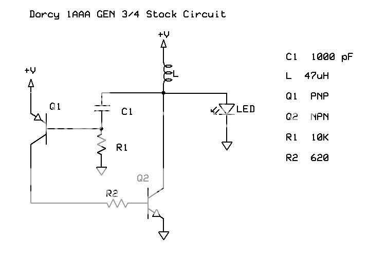
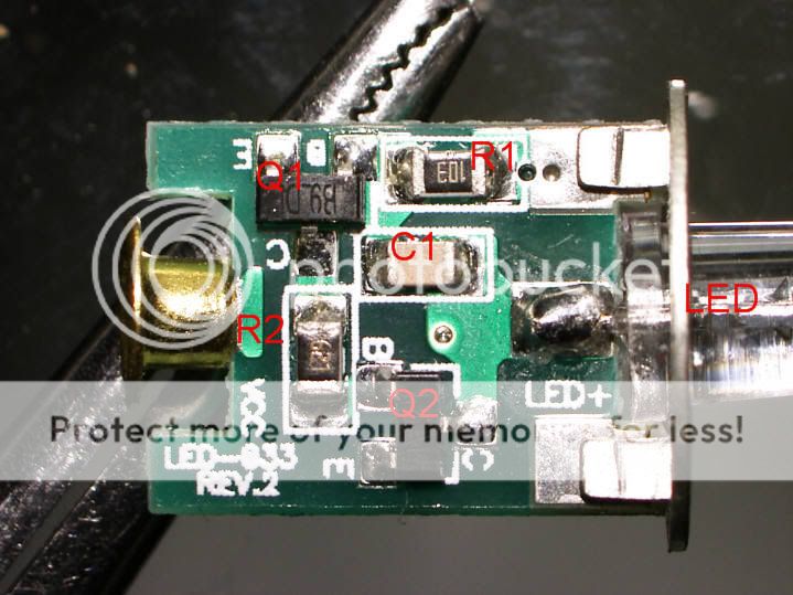
DorcyschGEN3Stock-1.jpg


dorcygen3_labeled.jpg


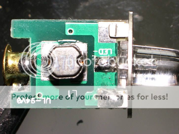
dorcygen3inductorside4mh_small.jpg

The images directly above were kindly provided by CPF member 1331.
If this circuit looks familiar to some of the oldtimers here, it should. Except for the specific component values, it is the same as the old Brinkmann 2AA LED light circuit that was much discussed a few years back and is drawn by member MrAl in this thread:
http://www.candlepowerforums.com/vb/showpost.php?p=658886&postcount=6
While MrAl's diagram for the Brinkmann version shows the inductor current being continuous (barely), as implemented in the Dorcy the inductor current goes to zero before Q2 turns on for input voltages below about 1.43V.
In common with the earlier Brinkmann circuit, the LED current is in the form of short, high current (up to 500mA peak!!!) pulses with the LED current being zero for the majority of the time. This is an extremely inefficient way to drive a 5mm LED which likely has a peak current rating on the order of 50-100mA.
This circuit is very mod friendly as the board is fairly spacious and there are a number of simple mods that will greatly enhance performance. I will be posting details of these mods over the next few days as time permits.
In the meantime, here is a review of three of these mods by CPF member UnknownVT:
http://www.candlepowerforums.com/vb/showthread.php?p=1804176#post1804176
 
Last edited:
This circuit works as follows.
When power is first applied, current flows from +V through the Emitter-Base junction of Q1 thus turning it ON. The voltage at the base terminal is now one junction Vf below +V or about 0.65V below +V. With Q1 on, current flows through Q1 emitter to collector through R2 and then through base to emitter of Q2. R2 establishes the level of the Q2 base drive current. Since Q1 is operating saturated, the Q1 Vce is negligible. Q2 base current, is thus about (+V-Vbe)/R2 or (+V-0.65)/R2. Current through the inductor and Q2 Collector to Emitter path rises from zero at a rate determined by the inductance and the available voltage across it. When the current has risen to where Q2 pulls out of saturation, the voltage at the collector of Q2 which has been rising only slightly with increasing current now rises sharply. Since the voltage across C1 cannot change instantaneously, this rise at the collector of Q2 also appears at the base of Q2 thus turning it OFF. With Q1 off, base drive current of Q2 falls to zero turning it OFF too. The voltage across the inductor now reverses polarity and rises pulling the node of Q2-C1-L-LED up rapidly until the LED conducts. The LED is powered by the additive sum of the cell voltage plus the inductor voltage. This will continue until the inductor current decays to zero. Meanwhile, while the inductor current is decaying powering the LED, the voltage at the base of Q1 (which had been pulled up to the LED Vf +(+V-0.65V) when Q2 turned off) has been decreasing as C1 charges through R1. If enough time were to elapse, Q1 would eventually turn back on even before the current in L falls to zero. With the component values as selected, the current in the inductor, L, falls to zero first. With the inductor current no longer decreasing (since it is zero) the voltage at the Q2-C1-L-LED node falls thus pushing the voltage at the base of Q1 down via C1 and turning it ON. The cycle is thus completed and begins again. The average input current is determined by the combination of the input voltage, the gain [called HFE] of Q2, and the value of R2. Higher Vin or HFE gives higher average current and lower R2 gives higher average current. While Vin is determined by the cell, we are free to chose Q2 with different HFE or R2 with different value.

This type of circuit has several types of inherent inefficiency. Since the LED is powered by brief, initially high current pulses, most of the power delivered to the LED is at rather high Vf. When Q2 first turns off the current through the LED is about 500mA with a fresh cell and the corresponding LED Vf is nearly 5V (!). This is a very inefficient way to operate an LED which was designed for a nominal 20mA continuous current.
The above inefficiency concerns the circuit output power to light conversion efficiency. The circuit also suffers from input to output power conversion inefficiency. The three largest contributors to input to output conversion losses from greatest to least are: 1) Q2 turn-off switching losses due to slow turn-off, 2) Q2 conduction losses via Vce while ON, and 3) resistive losses in the inductor.
In its stock configuration, Q2 turns off painfully slowly relative to the frequency of operation which is around 69kHz at Vin=1.2V. At a nominal Vin=1.2V it takes .746usec for the voltage at the collector of Q2 to rise from 1V to Vpeak. During this time the current is at its peak value and the LED cannot conduct until the voltage has risen enough to turn it on. Until then, the inductor current times the voltage across Q2 is pure power loss. Note that this circuit turns off Q2 just by removing its base current. The way to turn off this type of transistor quickly is not to just remove the current into the base but also to suck current out of the base. This is because there is capacitance internal to the transistor from its collector to its base. As the voltage at the collector rises, this capacitance tends to pull up the base voltage with it thus slowing the turn-off transistion. The greatest improvements to I/O power losses in the circuit lie in solving the long turn-off times for Q2. Lesser gains can be achieved by selecting a better Q2 with lower Vce saturation and/or the characteristic of pulling out of saturation more ''crisply''. The resistance of the stock inductor ranged from 0.39 to 0.45 ohms of three samples measured. In the stock configuration, inductor resistive losses are relatively low but would become increasing significant if the circuit is hotrodded to higher input power.
The modifications reviewed in this thread:
http://www.candlepowerforums.com/vb/showthread.php?t=149416
Address the above discussed inefficiencies to varying degrees.
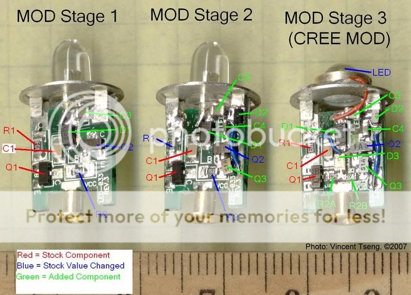
The ''Stage 1'' mod addresses the output power to light conversion inefficiency and also Replaces Q2 with a lower Vce sat transistor. R2 is adjusted to keep the input current unchanged from stock. The mod nets a gain in lm/w of 54% at a Vin of 1.2V.
The ''Stage 2'' mod incorporates the changes of ''Stage 1'' plus greatly speeds up the Q2 turn-off. Again, R2 is adjusted to keep the input current unchanged from stock. The mod nets a gain in lm/w of 105% at a Vin of 1.2V. And a gain of 267% at a Vin of 0.8V
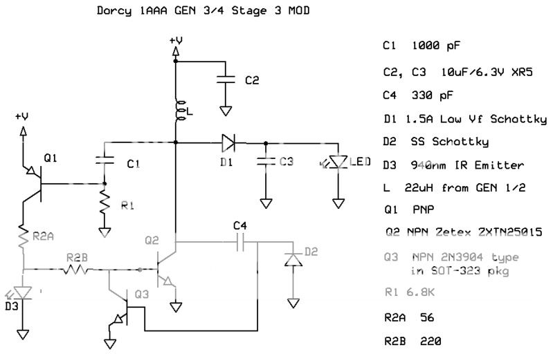
The ''Stage 3'' mod incorporates the changes of ''Stage 2'' and also attempts (with only slight improvement) to reduce the input current variation with Vin. This mod also more than doubles the average input current. The stock emitter has been changed to a P3 bin Cree XR-E.
Here are the circuits:
STOCK again:
DorcyschGEN3Stock-1.jpg

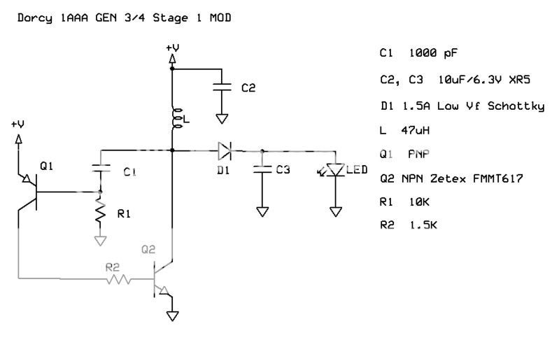
STAGE 1 MOD:
DorcyschGEN3stage1-1.jpg


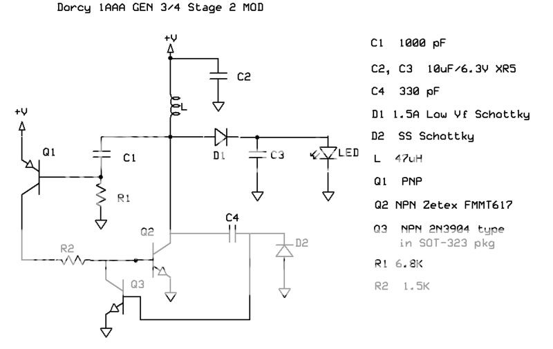
STAGE 2 MOD:

DorcyschGEN3stage2-1.jpg

STAGE 3 MOD:
DorcyschGEN3stage3-1.jpg


dorcy1mod_F_Labeled.jpg

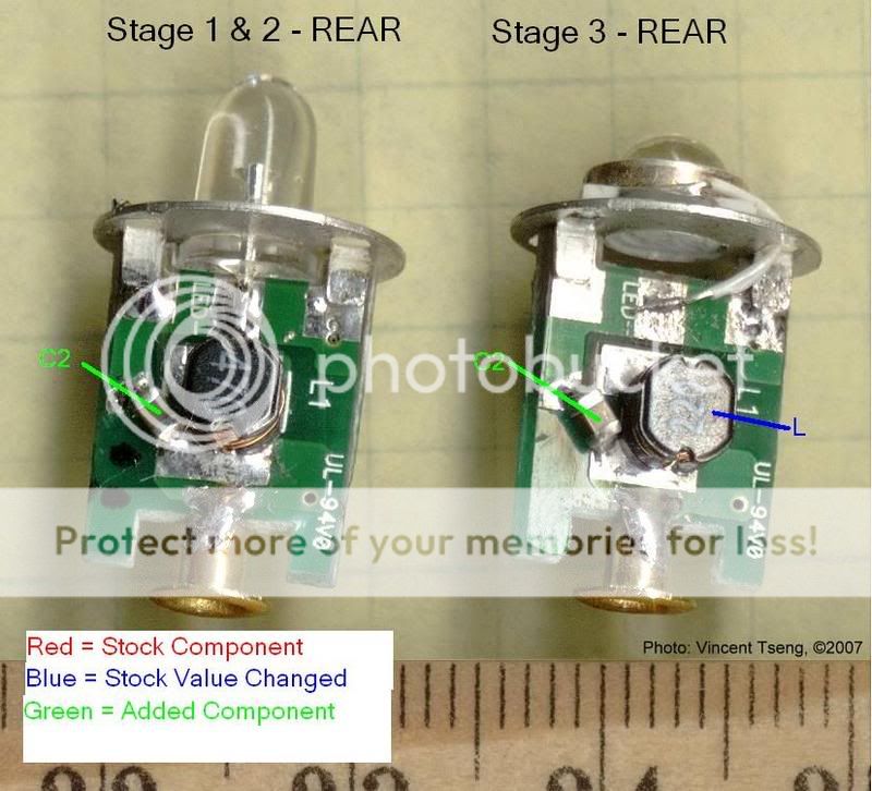
dorcy1mods_R_Labeled.jpg
 
Last edited:
Holy Smoke Doug that is some very complicated reading and I much admire you for even being able to figure it all out....can I ask you what your background is that you are so good with this technical stuff?

Also are all the parts you actually added to each circuit availabale from the older circuits or would I have to actually find them somewhere else? I have several of the older boards that I could remove parts from if I wanted to try any of this myself.
 
Robocop said:
Holy Smoke Doug that is some very complicated reading and I much admire you for even being able to figure it all out....can I ask you what your background is that you are so good with this technical stuff?

Also are all the parts you actually added to each circuit availabale from the older circuits or would I have to actually find them somewhere else? I have several of the older boards that I could remove parts from if I wanted to try any of this myself.

Robocop: R.e., your first question, I am an Electrical Engineer by training and worked most of my career as a Nuclear Test Engineer. About 13 years ago I became too lazy to work so I have just continually downsized my lifestyle rather than get a job. I'm now living in the space above a friend's garage. Other than lack of income, I've found no downsides to not working. It allows me plenty of time to dabble with whatever interests me at the moment.

Regarding your second question, with the exception of the 22uH inductor I salvaged off of an earlier GEN Dorcy for the Stage 3 mod, all of the parts used here are purchased for these modifications. All parts that you would need to purchase to do the Stage 2 mod come in at under $5 and are all available from one Electronics catalog retailer, Digikey. There are a couple of complications though if you are not already ordering parts from them for other reasons. There is a $5 surcharge for orders under $25 and shipping will run $5-8 depending on where you are. Also, some of the parts have a minimum purchase quantity of 10.

The idea of using these modifications as a tutorial project for folks that want to try their hand at modifications that require working with SMT components was discussed a bit in one of the other Dorcy 1AAA threads. If there is sufficient interest in this to where I likely won't be left holding the bag of parts I don't need, I could do a little mini-group buy of the parts, assort them into ''Kits'', and ship them for on the order of $5-6 for the first kit and well under $5 for a second since about $1.50 of the $5-6 figure includes the postage and packing costs. While this *may* be an inexpensive way to try your hand at working with SMT components, this assumes that you already have the minimal level of tools required. If you need to acquire lots of tools to do this, these could be very expensive lights indeed! On the other hand, you may be the sort that is always looking for a justification for buying new tools. If so, I, as well as others here, can help with recommendations for emptying your wallet on this project. If you have the inclination to buy off of Ebay, you can get an excellent soldering system for less that what some folks around here spend on a single flashlight. That system will still be excellent long after that flashlight is obsolete. How's that for a justification for redirecting some of your expenditures to quality tools?

Here is what I will do. I will keep the discussion of the Electronic/technical aspects of these mods here in this thread as I have a lot more to say. I will start a new thread in the Homemade/Modified subforum with the step by step ''nuts and bolts'' aspect of doing these mods as well as a bit of tutorial instruction for folks without much/any experience with hand soldering SMT components. I will include suggestions for minimal level of tools required. Based on that thread, folks can decide whether they want to give it a go and express interest in that thread in the form of ''I'd take a kit'' or ''I'd take X kits'' if done as a group buy. Once there appears to be a critical mass of interest I would start a group buy thread to handle the transaction stuff so that the Homemade/mod thread could remain focused on helping folks achieve success doing the actual mods. If there is interest I would be willing to include in the group buy effort a couple of inexpensive tool/supply items that some folks likely would need but are unlikely to be readily available locally or in small quantities [at the moment the two possible items that come to mind are scalpels and SMT solder paste]. Sound reasonable?
 
I do believe you are correct as to the entire costs involved in doing something as detailed as you have done here Doug. I have a simple 14 dollar soldering iron and a little bit of crappy solder bought at WalMart so for me it is just mostly interesting to read and look at your hard work rather than try to duplicate it...hehe

Most people myself included do not have the skills to work with such small parts and technical details so for you to attempt some form of group buy would probably not be practical however it is still very interesting.

I am curious as to why Dorcy did not simply offer this circuit with some of the more simple mods such as your stage one above. If the mass costs would be as low as you say it would most likely add 2 dollars or so to each light however performance would be greatly improved. Is it possible they simply did not know this circuit could be altered in such a cheap way?

Regardless your work on this is very facinating to me and I do appreciate all of the effort.
 
Robocop said:
I do believe you are correct as to the entire costs involved in doing something as detailed as you have done here Doug. I have a simple 14 dollar soldering iron and a little bit of crappy solder bought at WalMart so for me it is just mostly interesting to read and look at your hard work rather than try to duplicate it...hehe
Don't sell yourself short on learning new skills.

Robocop said:
I am curious as to why Dorcy did not simply offer this circuit with some of the more simple mods such as your stage one above. If the mass costs would be as low as you say it would most likely add 2 dollars or so to each light however performance would be greatly improved. Is it possible they simply did not know this circuit could be altered in such a cheap way?
Implemented on the scale of mass production, these modifications are way under a dollar in cost [excluding the Cree]. At the factory level the profit margin is likely way under a dollar. Since these lights sell in large quantities as they are currently designed and made, there isn't any economic sense in changes that increase production costs even by pennies.
 
Ok, here is how these mods work. I'll start with the simplest Stage 1:
DorcyschGEN3stage1-1.jpg

This modification added D1 and C3 to convert this to a more conventional step up switcher. The current received by the LED is now continuous with a small superimposed ripple at the circuit operating frequency. The LED operates more efficiently because it is not being subjected to the high current pulses of the stock circuit. Even with the added voltage drop accross the diode, the average voltage supplied by the inductor to the diode+LED is lower than to the LED alone in the stock circuit. Because the stored energy in the inductor is used to produce lower voltage it thus provides more average current. The average current to the LED is thus higher than the stock circuit for the same amount of stored energy in the inductor. Q2 was changed to a Zetex FMMT617 which has lower Vce saturation under the same operating conditions as the stock circuit. With a Vin=1.2V, scope measurements of Vce during the Q2 ON period at 50% of the ON interval read 0.13V and at 90% of the ON interval read .27V with the stock Q2. Similar measurements with the FMMT617 are 0.065V and 0.13V. Exact gain in output from this is not readily calculated due to the non-linear nature of what's going on but is likely around 10% or so. The only other change in the Stage 1 mod is the addition of the input filter capacitor, C2. If the power supply were a perfect zero impedence source, the addition of C2 would accomplish nothing. With a real world cell, it allows the cell energy to be utilized a bit more efficiently by smoothing the input ripple current. It does the most good for nearly depleted alkaline cells which have high internal resistance but has negligible benefit for NiMh or L92 Eveready lithiums which have relatively low internal resistance.
This modification does nothing to address the Q2 losses from slow turn-off.
 
Last edited:
The stage 2 mod incorporates the changes of the Stage 1 mod plus adds a Q2 turn-off speedup circuit comprised of added components C4, D2, and Q3.
Stage 2:
DorcyschGEN3stage2-1.jpg

The value of C4 is not critical and was tested with values ranging from 100 to 470pF with essentially equal performance. D1 is a small signal [SS] schottky diode, and Q3 can be any reasonably fast NPN SS transistor. For Q3 I used a 2N3904 type in a SOT323 package.
The speedup circuit works as follows. As the voltage at the collector of Q2 starts to rise as it starts to turn off, this rise causes voltage at the base of Q3 to also be pulled up via C4. As soon as the base of Q3 reaches it's turn on voltage of around 0.6V, Q3 turns on and pulls the base of Q2 to ground causing Q2 to turn off rapidly because it 1) discharges the transistor's internal base-emitter capacitance and 2) provides a path for the transistor's collector-base capacitance to charge as Q2 to turn-off; without this path, the current to charge the collector-base capacitance flows through the base-emitter junction which slows the turn-off. D2 is required to discharge C4 when Q2 turns back on later in the cycle. Without D2, C4 would permanently maintain a charge and the speedup circuit would only work on the first cycle. This circuit is very effective. It reduces the Q2 turn-off 1V to Vpeak time from .75usec [stock] down to 0.02usec [with speedup]. This eliminates almost all of the loss associated with the Q2 turnoff. This benefit enables some other viable modifications such as lowering the inductor value [which has the consequence of raising operating frequency] to achieve lower inductor resistance. In the stock circuit, the increased Q2 switching losses due to higher operating frequency will more than offset any loss reductions from the lower resistance of substituting a lower value inductor. BTW, I measured the resistance of the stock 47uH inductors in the range of 0.39-0.45 ohms. The 22uH inductors found in the Gen I Dorcies measure in the range of 0.20-0.25 ohms and thus would be a good substitution if one were to increase the input current greatly by reducing the value of R2. At stock or only moderately increased input current the benefit is small and not worth the effort.
Here is some comparitive power input to output efficiency data with the speedup circuit enabled and disabled.
Code:
Vin     %Eff-enabled   %Eff-disabled 
0.71      63.7               0 
0.8       75.3               17.6 
0.9       77.9               41.0 
1.0       79.3               53.2 
1.1       79.2               59.6 
1.2       79.1               60.9 
1.3       79.5               57.5 
1.4       80.6               53.5 
1.5       81.0               50.7
It is clear from the above that the Stage 2 mod will provide not only more output for the same input power but compared to the Stage 1 mod will provide much extended low output runtime when the cell is mostly depleted.
For comparison, here is some power input to output efficiency data pulled from the old thread that is linked in the first post of this thread. The ''CX'' IC was the one used in the Gen I Dorcies and the ''AM50'' IC in the Gen II Dorcies.
Code:
CX=GEN I data: 
Vin  Iout[mA]  Eff[%] 
.50  4.3         66.5
.70  8.4         66.8
.90  15.2       69.4
1.1  23.4       70.6
1.2  34.4       72.4
1.3  53.0       70.5
1.5  95.6       67.7 
AM50=GEN II data: 
Vin   Iout(mA)  Eff[%]
.90   19          67.7
1.0   25          68.0
1.1   39          65.0
1.2   53          61.3
1.3   66          57.6
1.4   78          53.6
1.5   89          49.5 
And for a final comparison, some data for the ARC AAA from the ARC LLC days. 
I don't know whether this is the same circuit as the current generation of 
ARC AAA:  
Vin(V) Iin(mA) Vout(V) Iout(mA) Eff(%) 
0.203  15.55     2.78      0.64      56.5 
0.503  42.7      3.02      4.3       60.6 
0.803  76.8      3.22     12.0       62.7 
0.898  90.2      3.27     15.7       63.3
0.998  101.7     3.32     19.6       64.2 
1.102  118.4     3.37     25.0       64.6 
1.202  168.7     3.47     36.4       62.3 
1.280  198.0     3.47     39.1       53.5 
1.393  180.0     3.49     41.6       57.9 
1.500  172.4     3.51     44.6       60.6 
2.00   145.2     3.59     57.9       71.5 
3.00   158.6     3.79    106.5       84.9
 
Last edited:
I edited the schmatics to correct errors: I had the LEDs pointed the wrong way as well as the IR emitter in the Stage 3 mod. While it may look funny, D2 in the stage 2 and 3 mods *is* oriented correctly.
 
Heads up for those who may have found some of the earlier posts it this thread a bit deep. This post explains a very useful concept and requires no more prior knowledge than an understanding of Ohms Law.

The circuits used in the ARC AAA and the Gen I and II Dorcies are capable of operating down to less than 0.2V. See the ARC data table a couple of posts back. Somewhat counterintuitively, this makes them perform less well than the Stage 2 and 3 mods that cannot operate below about 0.6V. The ARC and the Gen I and II Dorcies circuits all use a CMOS based stepup switching regulator IC that powers itself off of it's output voltage. These ICs need about 0.7V to startup but once running can continue to operate down to almost zero volts as long as the output voltage can be maintained high enough to power the IC. On a very depleted cell this characteristic causes most of the cells remaining energy to be expended as heat in the cell.
Here is a little tutorial:
The most common and simple model for a cell is to combine an ''ideal'' cell with an internal resistance, Ri. An ideal cell has a voltage V and can provide up to infinite current while maintaining the same voltage. It is the internal resistance Ri that makes the model somewhat more real as the terminal voltage of the model will droop with increasing current due to the voltage drop across the Ri. This model is far from perfect but is adequate for this discussion. One of the first things a Freshman electrical engineering student learns is that the maximum power that can be withdrawn from a DC source with internal resistance, e.g., our cell model, is under the condition that the external load resistance, R Load, equals the source internal Ri. Under these conditions exactly half of the power from the ideal source is dissapated in the internal resistance, Ri, and the other half in the load, R Load. If the value of R Load is reduced, even though the ideal source will yield more power, the external load receives less and the internal resistance dissapates more. This is exactly what happens with the ARC AAA and Dorcy Gen I and II circuits powered by nearly depleted cells. Let's look at a couple of examples. See below:
Cell_RiRL_small-1.jpg

While a fresh alkaline cell has an open circuit voltage of 1.56V, the value V in our model, and an internal resistance of a fraction of an ohm, Ri in our model, a nearly depleted cell can have a V around 1.1V and an Ri of 100 ohms.
Now let's use these values in the equations above. To get maximum power to the load, R Load = Ri = 100 ohms. Using these values in the equation for I

I = 1.1V/(100+100) = 5.5mA

The voltage across the load from the next equation is:

(5.5mA)(100 ohms)=0.55V or exactly one half the ideal cell voltage.

Power to the load is IxV = 5.5mA x 0.55V = 3.03mW

Now look what happens if we make R Load = 10 ohms. Current is now:

I = 1.1V/(100+10) = 10 mA

Voltage across the load is:

(10mA)(10 ohms) = 0.1V

Power to the load is 10mA x 0.1V = 1mW

You can see that we are drawing almost twice the current but receiving just under a third the useful power.

Now lets look at the opposite direction. Make R Load = 200 ohms:

I = 1.1V/(100+200) = 3.667mA

Voltage across the load is:

(3.667mA)(200 ohms) = 0.733V

Power to the load is 3.677mA x 0.733V = 2.7mW

So by drawing less current than the previous example, we get more useful power to the load.
It is exactly because the Dorcy Gen 3/4 circuit cannot pull the cell voltage below about 0.6V that this makes them perform much better than the ARC and the Gen I and II Dorcies circuits on depleted cells provided that the ''overhead'' losses are reduced as they are by the stage 2 and 3 mods.
This characteristic accounts for why Vincent finally gave up on doing a runtime test at 40 hours in this thread:
http://www.candlepowerforums.com/vb/showthread.php?t=149416
It is noteworthy that a significant fraction of the total potential energy in an alkaline cell is only available at rather low discharge rates.
The link below is to the lastest version of the Eveready alkaline AAA datasheet:
http://data.energizer.com/PDFs/E92.pdf
Take a close look at the bar graph on the right side of page one. It shows the mA-Hr capacity that can be withdrawn from the cell down to a final voltage of 0.8V. At a drain of 400mA it appears that you can get around 450mA-Hr but at a drain of 25mA you can get around 1250mA-Hr, or about three times as much. So what happens to the rest to the capacity [ampacity] if you pull 450mA-Hr out at a rate of 400mA? Is it lost forever? No. It is still there but is just not accessible at a high continuous rate. You can get a bit of it at a high rate if you allow the cell to rest as Vincent has shown or you can get all of it if you are willing to accept it at an decreasing maximum rate of withdrawal. With alkaline cells the performance of the drive circuit with nearly depleted cells has a big impact on the ''moon mode'' performance. With NiMh cells it is of much less importance since NiMh can deliver almost their entire capacity at relatively high rates. One conclusion should be evident about the maximum ''reasonable'' current drain from an alkaline cell in a light like this: it depends upon whether the intended use is intermittant or continuous. The last graph on page two of the above linked datasheet shows that even at a relatively high 600mA rate, about 750mA-Hr can be withdrawn if the usage is an intermittant 10 sec/min 1 hour/day. Interestingly, the alkaline cell runtimes done by CPF member Silverfox use a minimum discharge rate of 0.5A. At this rate, the discharge test terminates with less that half of the total potential energy taken from the cell.
Major edit: New material
Our CPF battery testing guru, Silverfox, has kindly performed some testing in support of this subject. He discharged an alkaline AAA at 0.5A down to 0.5V and then continued at 0.1A and then finally at 0.01A.
You can see from this graph that less than half of the Ahr and Whr are extracted in the 0.5A discharge.
DuracellCTAAARepeatStudy.gif

This has significant implications for convertor performance when the battery is partially discharged. A converter that tries to withdraw more power that the cell can provide will waste most of the remaining energy in the cell and produce a sharp rolloff in light output such as in the following graph:
Fenix%20L0D%20CE%20-%20medium.png

A convertor that uses the remaining energy more efficiently by drawing decreasing current will produce a more gradual rolloff in output such as in the following graph:
Fenix%20L1P%20V2.5%20vs%20Civictor%20V1.png

Runtime graphs provided by CPF member chevrofreak.
Many folks would look at the first graph and see it as ''good regulation'' without realizing that it is achieved by failing to utilize a lot of residual energy towards the end.
 
Last edited:
Doug S wrote: "It is clear from the above that the Stage 2 mod will provide not only more output for the same input power but compared to the Stage 1 mod will provide much extended low output runtime when the cell is mostly depleted."

This is EXACTLY why I was so impressed with Doug's Stage 2 mod -

Proof of the pudding etc - it's now my EDC -

and because I am so pleased with it -
I have done a separate full comparison review of the Stage 2 mod -

Dorcy 1AAA gen4 - Doug S Stage 2 Mod

with this Stage 2 mod I am now a full "convert" to the Dorcy 1AAA Spot beam - this is not an easy thing - since, like most, I had an unhealthy bias/prejudice against Spot beams......

ref: thread on all 3 mods -

Dorcy 1AAA gen4 Mods

My BIG thanks to Doug S for doing these mods and for allowing me to get my close to ideal EDC light in the stage 2.
 
In this post I discuss the stage 3 mod and what I was trying to accomplish.
The stock circuit as well as the prior generation Dorcies, the ARC 1AAA and the stage 1 and 2 mods all share the characteristic of being unregulated circuits in the sense that input power varies with input voltage. Input current and thus input power rise with increasing input voltage. The Stage 3 circuit attempts with some limited success to limit the rise of input current with input voltage. Even if input current were held entirely constant, input power would still rise since power is the input current multiplied by the input voltage. Look at the following table in which I have measured the input power vs input voltage for two versions of the Stage 2 circuit with R2=1K and R2=1.5K. I have normalized the data to P=1.0 at a Vin=1.2V for each of the two circuits. Note that Pin varies strongly with Vin and for Vin above 1.2V the problem is worse for the higher powered R2=1K circuit. I have other test data that shows the problem continues to worsen at higher powers [lower values of R2].
Stage 2 with R2 = 1K and 1.5K, Power normalized to 1.0 at Vin=1.2V
Code:
         R2=1K      R2=1.5K 
Vin     Pin           Pin 
0.8     0.22         0.12  
0.9     0.36         0.37 
1.0     0.55         0.55 
1.1     0.76         0.76
1.2     1.00         1.00
1.3     1.28         1.25
1.4     1.59         1.51
1.5     1.93         1.80

Below is the Stage 3 circuit.

DorcyschGEN3stage3-1.jpg


Unlike the stock, stage 1, and stage 2 circuits in which the base resistor R2 of Q2 is essentially powered from +V [there is very little drop through Q1 when it is ON], in the stage 3 circuit R2 is driven by a semi-stable voltage [about 1.05V] derived from using a 940nm IR emitter as one would use a zener diode. The IR emitter, just as other types of forward biased diodes such as an LED, has a voltage drop across it that varies only slightly with current. In the case of this IR emitter, it has a Vf of about 1.05V at a fraction of a ma and increases by 0.03V per doubling of current. Since it cannot conduct any appreciable current below 1.05V it is only helpful at higher input voltages.
It does help somewhat but not as much as would be desired. I don't have a proper comparison between a Stage 2 and a Stage 3 set up for the same power. The best I have is a comparison of a Stage 2 with R2=1K which gives a power of 155mW at Vin=1.2V and a Stage 3 with R2A=100, R2B=470 which gives a power of 213mW at Vin=1.2V. Again, powers are normalized to that at a Vin=1.2V
Code:
       Stage 2    Stage 3
       R2=1K      R2A,B=100,470 
Vin     Pin           Pin 
0.8     0.22         0.22  
0.9     0.36         0.37 
1.0     0.55         0.57 
1.1     0.76         0.79
1.2     1.00         1.00
1.3     1.28         1.17
1.4     1.59         1.37
1.5     1.93         1.49
As expected, there is no significant benefit at and below Vin=1.0V. There is some modest benefit for higher voltages. At even higher power stage 3 where R2A=56, R2B=220 yielding Pin=346mW at Vin=1.2V [this is the one that Vincent tested] the rise in Pin with Vin is no better than the stage 2 circuit with R2=1K. Data below:
Code:
       Stage 2    Stage 3
       R2=1K      R2A,B=56,220 
Vin     Pin           Pin 
0.8     0.22         0.23  
0.9     0.36         0.42 
1.0     0.55         0.65 
1.1     0.76         0.90
1.2     1.00         1.00
1.3     1.28         1.48
1.4     1.59         1.72
1.5     1.93         1.95
There is clearly room for improvement on the problem of making the Pin a bit more regulated with Vin. I know what I will try next but that will need to wait for a later date. I first want to do a ''how to do it'' thread over in the Homebuilt/Mod subforum. I will show all three mods. I believe, however, at this point the Stage 2 is the best result for the effort expended. The Stage 2, of course can be combined with changing out the emitter to something else. This will be my last post to this thread with the exception of answering questions that may be posted into this thread.
 
Given the title of this thread, I suppose I should give performance data for a stock circuit. The data below is an unmodified Gen 3/4 and is the actual unit that was later modified into the Stage 2 that was reviewed by Vincent in his review thread. The Φ and Φ/W columns are a relative measures of lumens and lumens/Watt input power but are not calibrated values, i.e., are good for relative measurement comparison only.

Code:
[B]Stock[/B]
Φ/W    Φ     Vin    Iin(mA)   Pin(mW)  Freq(kHz)   LED Vpk  
39.2   1.1   0.801   35.0       28.0        136.6        3.33 
67.6   3.2   0.901   52.5       47.3        105.1        3.68 
96.2   4.7   1.000   68.6       68.6         89.1         3.87 
70.2   6.6   1.102   85.3       94.0         77.6         4.10 
67.7   8.2   1.200   100.9      121          69.4         4.26 
65.6   9.9   1.300   116.2      151          63.3         4.44 
62.3  11.4   1.401   130.7      183          58.5         4.58 
60.0  13.1   1.500   145.5      218          55.0         4.72 

[B]Similar data for the ''as modified'' Stage 2 [/B] 

Φ/W       Φ      Vin      Iin(mA)   Pin(mW)  Freq(kHz) 
143.7     2.5    0.803    17.4       14.0        70.1 
163.9     7.2    0.900    48.8       43.9       108.4 
158.8    10.5   1.002    66.0        66.1        92.4 
147.1    13.4   1.103    82.6        91.1        80.8
138.6    16.6   1.202    99.6       119.7        71.4 
130.9    19.6   1.302   115.0       149.7        64.4 
118.5    22.0   1.400   132.6       185.6        59.3 
111.6    25.2   1.502   150.3       225.8        54.9
 
Last edited:
Sorry for the delay in the questions but I lost this thread and was not able to find it until 'A classic revisited Dorcy 1AAA' resurfaced and I can link in.

I gave my Gen3 board/LED away before I used it much. Is the 'frequency of operation which is around 69kHz' noticeable?
Doug S said:
In its stock configuration, Q2 turns off painfully slowly relative to the frequency of operation which is around 69kHz at Vin=1.2V.

Can the diode D1 and capacitor C3 in the stage 1 mod be used to smooth out other types of pulsing output to the LED. I am thinling of the massive amount of whining about the flicker of PWM circuits.
Doug S said:
The ''Stage 1'' mod addresses the output power to light conversion inefficiency and also Replaces Q2 with a lower Vce sat transistor. R2 is adjusted to keep the input current unchanged from stock. The mod nets a gain in lm/w of 54% at a Vin of 1.2V.
STAGE 1 MOD:
DorcyschGEN3stage1-1.jpg
 
.
LEDninja said:
Upon further reflection, I've given you some misleading info. While the answer to your second question is in fact yes, if the frequency is low enough to be bothersome, the value of C3 will need to be quite large to acheive the desired effect; large enough to be impractical in some instances.
 
Top