So i killed my new Seoul P7... (updated: Just wounded...)

IMSabbel

Enlightened
Joined
Dec 4, 2004
Messages
921
... and it was a _really_ nice daylight tint, too. And all 4 dies were perfectly the same brightness, even at very low intensities. I ruined the perfect P7, just to rig a quick demo off my PSU to impress people at work. Damn

I just underestimated those trustfire 18650 cells. One in direct drive (on a good heatsink) was pretty bright.
Then i thought: Maybe two in parallel might be brighter (less internal resistance).

Well, it turned out that mine had a very low Vf, too (i idiot even meassured it before, i hit 4A at 3.905V at the psu, minus probing head contact resistance this is more like 3.8V.

And those were fresh 18650.
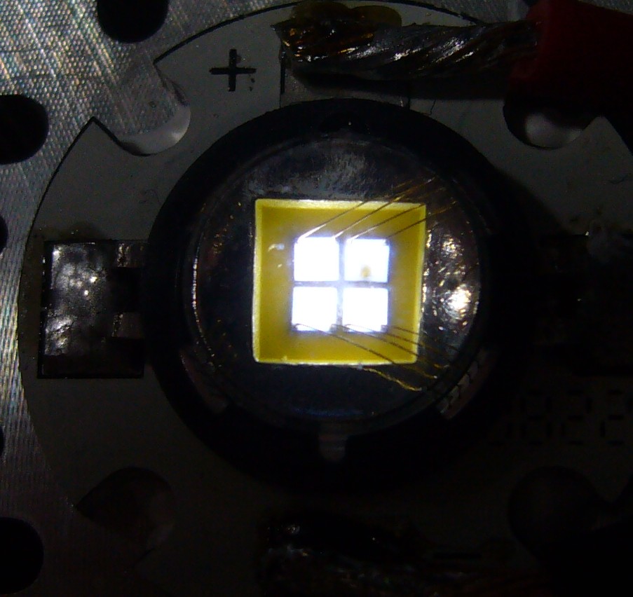
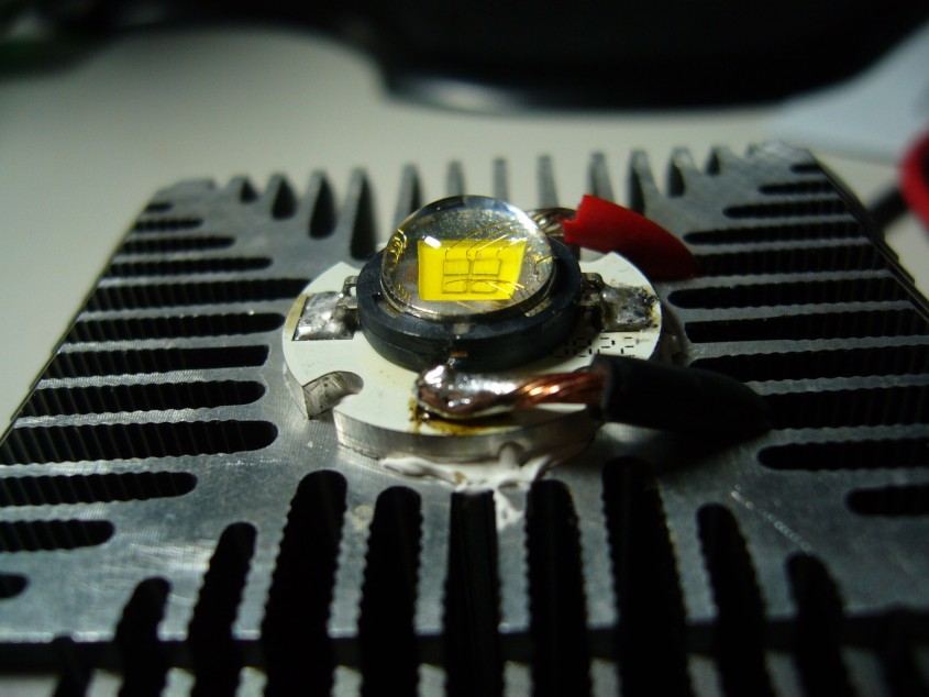
To make a long talk short, it seems my P7 had a very near dead experience, with a very curious failure mode:

A dark spot on one of the dies, plus a 20 Ohm parasitic resistence path ( i get 100mA at 2V, where i got non before).
It seems the bonding wires are all fine, so the question is: How did it fail? Electromigration creating a conductive path through the die?

Pics and a video to follow...
 
Last edited:

IMSabbel

Enlightened
Joined
Dec 4, 2004
Messages
921
Re: So i killed my new Seoul P7... (and other stuff)

Ok, here some pics.
First the Led on the heatsink. This was a Thermoengine HSF from a company called thermionics, IIRC. If anybody still has some of them lying around (they are back from the athlon days), i would be more than ready to buy them off....
The center column is perfectly the right size of a star...

hs-top.jpg

hs-bottom.jpg


Here a shot of the led itself. I like the star. Its a lot more solid than the XREs and solid aluminium with only a _very_ _very_ thin layer of PCB on top. With that 2mm or so thickness, spreading of heat before the thermal transfer through the thermal glue should be no problem at all.
p7-off.jpg


And here is how it looks like when powered up. On about 2.5V, obviously, or it would be completely white :)

p7-spot.jpg
 

IMSabbel

Enlightened
Joined
Dec 4, 2004
Messages
921
Re: So i killed my new Seoul P7... (and other stuff)

A Youtube video of the voltage ramp. Sadly, its worse than it was before the defect. You get this leaking current (120-150mA offset), and a higher Vf (i guess its only a 3.67 die led now...)

Before, i hit 4A at just below 3.9V with a cold led (substract about .1V for the probing heads).

But still, nice to see how much it still increases in brightness after 2.8A, even in the damaged state.
I will order an replacement. When this is arrived, i will pump it up till the P7 dies completely. The 10 Ampere of the PSU should be more than enough...

http://www.youtube.com/watch?v=R77Z9qfCKm8

If somebody want to read the display of the PSU, here a link to the higher res divx file
http://bilder.markusweigand.de/bilder/flashlight/p7/P1030621.avi
 

kris23

Newly Enlightened
Joined
Jun 7, 2008
Messages
109
Re: So i killed my new Seoul P7... (and other stuff)

sorry to hear that, any plans to get a new one?
 

IMSabbel

Enlightened
Joined
Dec 4, 2004
Messages
921
Re: So i killed my new Seoul P7... (and other stuff)

sorry to hear that, any plans to get a new one?

Yeah. That was was just a tester, too.

But i doubt i will get another one that good again...
But $23 is less than a luxon was not that long ago, so i will order me a couple to replace my desk lighting.
 

MrGman

Flashlight Enthusiast
Joined
Feb 6, 2007
Messages
1,777
Re: So i killed my new Seoul P7... (and other stuff)

The 4 die are in parallel electrically, the one die with the dark spot on it was probably the one with the absolute lowest Vf and was drawing the most current. They do not all current share equally 100%, not possible, especially at high power levels. It got the hottest and started to reflow the substrate of that chip. that chip is now drawing leakage current because the p/n junction inside of it has been degraded by havling reflowed semiconductor material that is no longer in a crystalline lattice structure. Even though you had it on a massive heatsink, you didn't have airflow over it to help maximum transfer out of the die, I am guessing not. You were putting very nearly 16 watts into the quad dice. So looks like you found the limit. Even though your star is on the heatsink, its thermal transfer capabilities are limited. If you had that heatsink sitting on a nice block of ice it would have helped but still there are limits and you now know you can't pump 16 watts through a P7.

It was murrrrrrrdderhhhhhhhh!.

My guess is that if you were able to severe the bond wires to the one die with the dark spot the leakage current would go away.
 

IMSabbel

Enlightened
Joined
Dec 4, 2004
Messages
921
Re: So i killed my new Seoul P7... (and other stuff)

The 4 die are in parallel electrically, the one die with the dark spot on it was probably the one with the absolute lowest Vf and was drawing the most current. They do not all current share equally 100%, not possible, especially at high power levels. It got the hottest and started to reflow the substrate of that chip. that chip is now drawing leakage current because the p/n junction inside of it has been degraded by havling reflowed semiconductor material that is no longer in a crystalline lattice structure. Even though you had it on a massive heatsink, you didn't have airflow over it to help maximum transfer out of the die, I am guessing not. You were putting very nearly 16 watts into the quad dice. So looks like you found the limit. Even though your star is on the heatsink, its thermal transfer capabilities are limited. If you had that heatsink sitting on a nice block of ice it would have helped but still there are limits and you now know you can't pump 16 watts through a P7.

It was murrrrrrrdderhhhhhhhh!.

My guess is that if you were able to severe the bond wires to the one die with the dark spot the leakage current would go away.

Well, i wouldnt be so negatice.
Lack of ventilation isnt the problem. The heatsink became never very hot, even touching right next to the led after 20 minutes of 2.5A. My guess would be about 45 C.

What killed it was direct driving it getto-style with two parralel 18650. My guess from meassuring those cells is that i have been driving it with well over 5 Ampere at that point.
My guess is that yes, this die was the one with the lowest Vf, and the current density became high enough locally to create a "bridge" by elecromigrating crap into the semiconductor. As soon as this increased the conductivity, things went to hell...


Actually, I consider the fact that the bond-wires didnt flash to be very nice...
I am sure i can push the whole thing the 6Amps or so when i kill it.

But boy, this thing is bright. A lot of my colleques saw spots this afternoon :D
I should have been alarmed by the brightness (it went up at least 25% going from one 18650 to 2 18650 in parallel). But there was lots of daylight coming in, so it didnt _seem_ that bright. Even though it was casting shadows on the ceilign without any reflector.
I must have easily pushed 1000 lumens out of it with that stunt...
 
Last edited:

IMSabbel

Enlightened
Joined
Dec 4, 2004
Messages
921
Re: So i killed my new Seoul P7... (and other stuff)

Seems the lights are sturdier than it seems:

I set my PSU to 2.8A, and let it run the whole workday.
No futher damage or degration visible.
So i guess i just downgraded the LED from C-bin to B-bin (and make it useless at very low power, but for that i wouldnt want a P7 anyways).

Btw, after 8 hours at 2.8A, the heatsink shown above had about 45-50C hot, but touchable, at the other end of the solid aluminium rod. Taking all the other temperature gradients into account, this should mean a junction temperature of just above 100C (calculating conservatively).
So not perfect for optimal brightness, but according to the specs perfectly fine.
 

MrGman

Flashlight Enthusiast
Joined
Feb 6, 2007
Messages
1,777
Do you have the thermal resistance numbers of the star that the die is on?
 

IMSabbel

Enlightened
Joined
Dec 4, 2004
Messages
921
No. I dont. But the star is pure aluminium, with very thin (i would guess <50um) pcb layer on top. So i dont think its significant vs the 3.5 K/W of the P7 itself.

But i can do a direct comparison, soon.
because the promising results from the P7, i have ordered 4 of them without the star for a special project...
 
Top