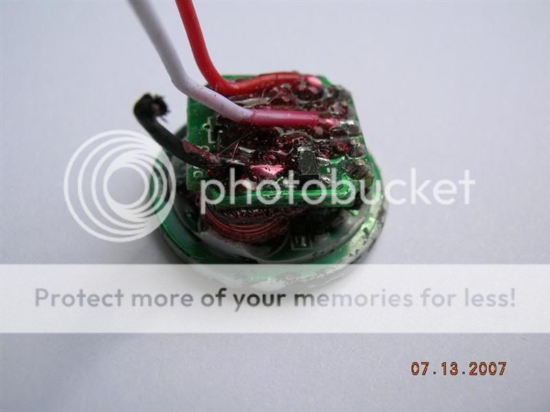
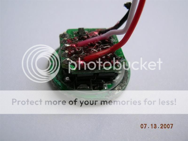
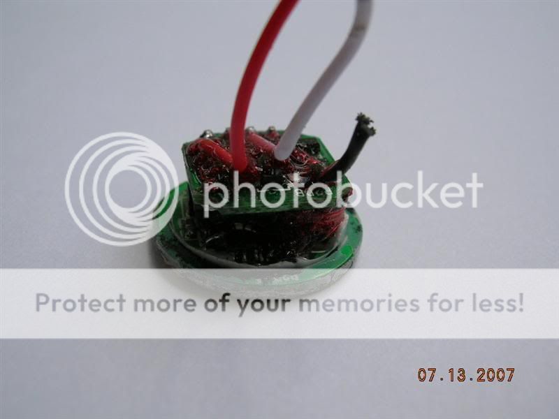
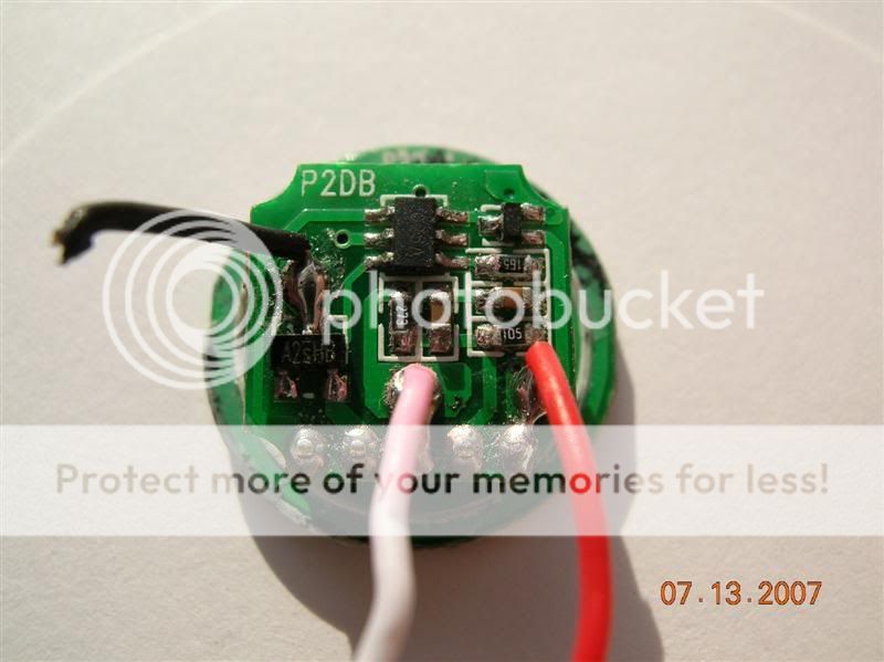
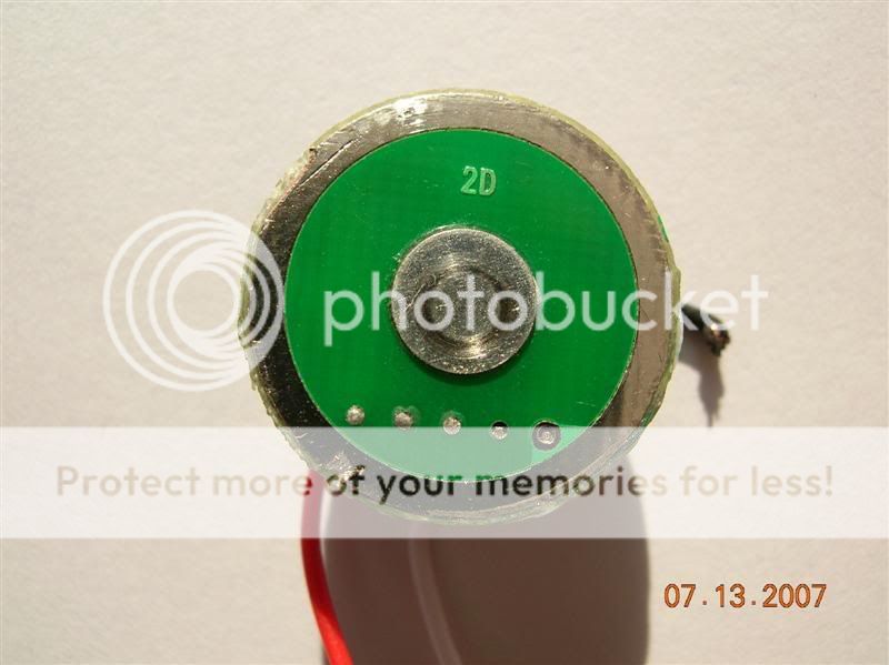
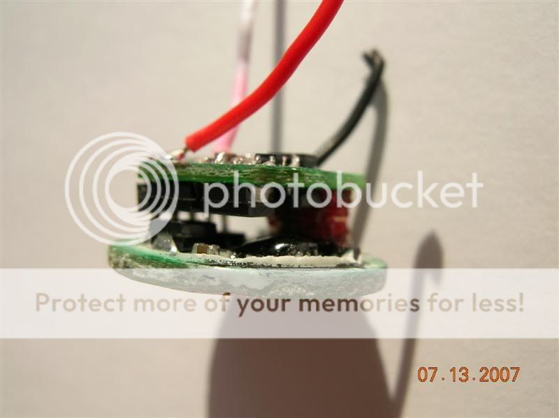
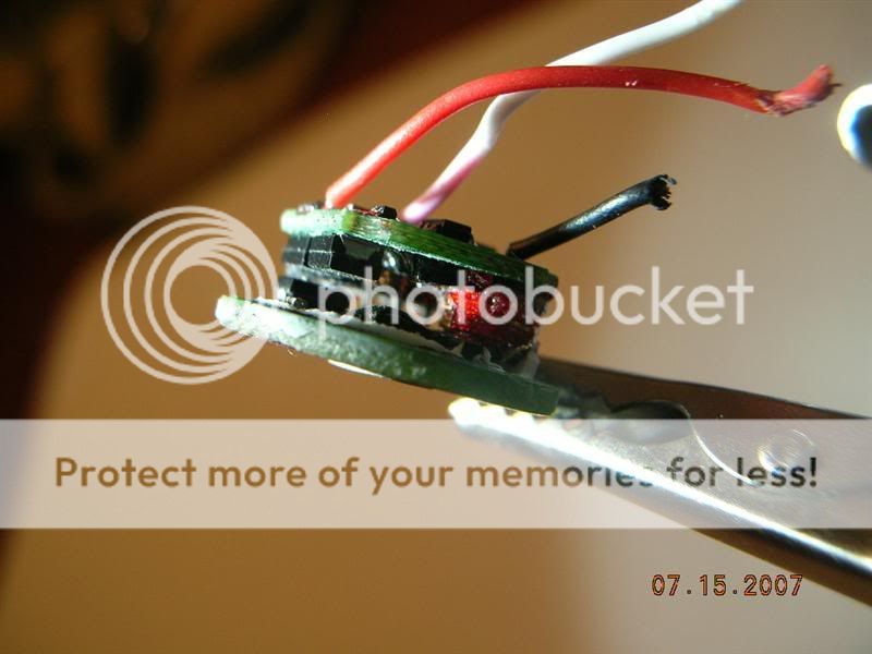
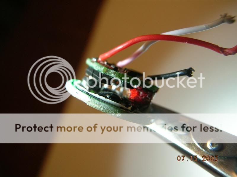
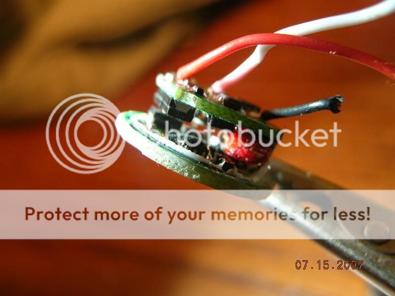
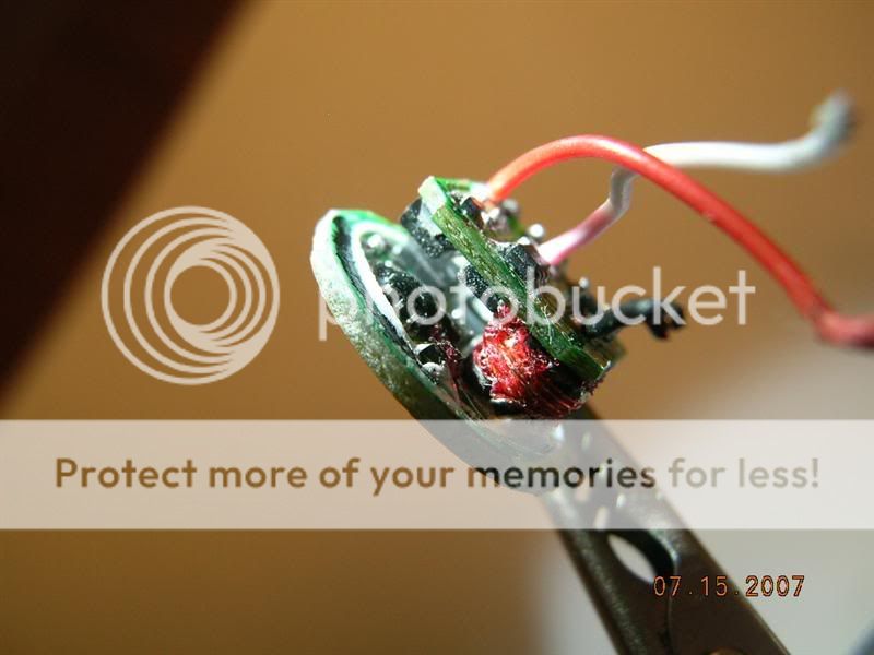
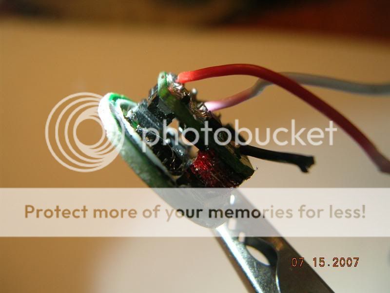
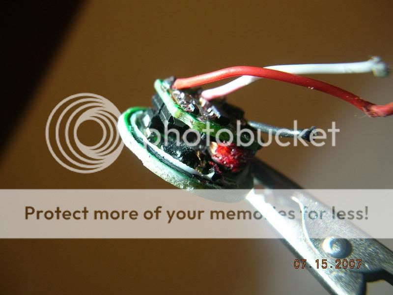
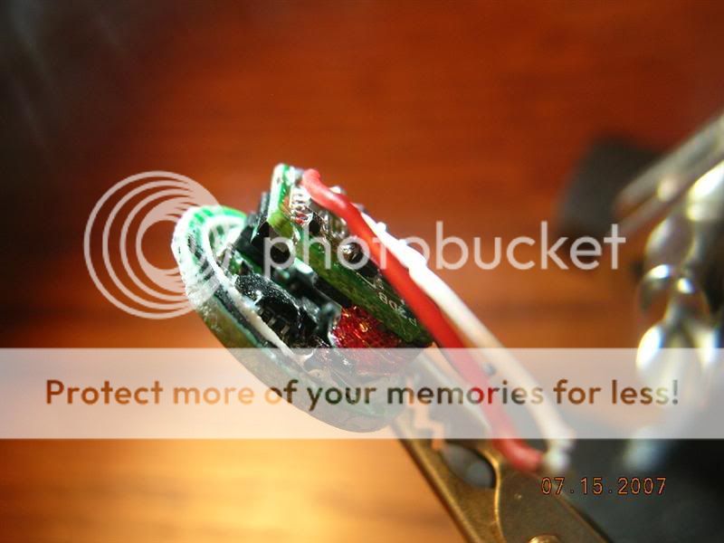
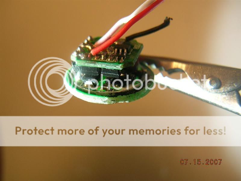
Fenix LxD/P2D boost driver revealed. 7/16: more (good) pictures of inside the driver.

wintermute

Enlightened
Joined
Nov 16, 2004
Messages
681
Well qip sent me his murdered LxD head. The little wires dropped through the hole and were unrecoverable. So, I asked qip for the head so I could try to get the circuit out and maybe do some testing. So...after an hour or so thinning out metal with a dremel and giving myself a couple blood blisters when trying to bend little bits of metal out of the way of the PCB - I extracted the LxD/P2D boost module intact. Here are the pictures:
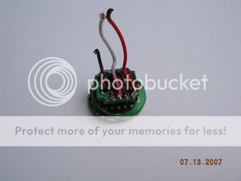
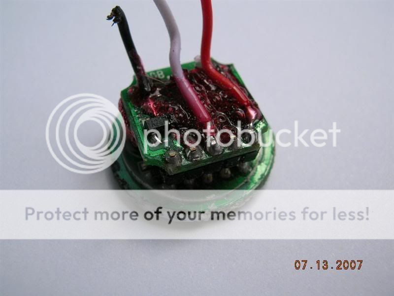
DSCN4070Medium.jpg


DSCN4071Medium.jpg


DSCN4072Medium.jpg


DSCN4073Medium.jpg


DSCN4074Medium.jpg


I am going to go to work with some toothpicks and such to get the red goo out of the way before the next pics - but wow, I have to say, Fenix does not want users servicing their own lights. I can't imagine how anyone could get this thing out intact without killing the head as we did.

More to come. :twothumbs
 
Last edited:
Re: Anyone wonder what a Fenix LxD/P2D boost circuit looks like?? (pics inside)

Red goo looks like it would make the PCB pretty moisture proof - and maybe provide a little shock protection as well...

Loss of "user" serviceability is a pretty reasonable tradeoff for improved reliability, from the view of the manufacturer.
 
Re: Anyone wonder what a Fenix LxD/P2D boost circuit looks like?? (pics inside)

Good job getting that bad boy out of there :thumbsup: must have been fun
 
Re: Anyone wonder what a Fenix LxD/P2D boost circuit looks like?? (pics inside)

It would be great if you could measure it's efficiency in different modes.

Also would be interesting to see what boost converter and microcontroler they are using?
 
Re: Anyone wonder what a Fenix LxD/P2D boost circuit looks like?? (pics inside)

Any tips on getting rid of the red goo? Does heat work to soften it up??

As far as the testing goes - my testing will have to be limited at this time, simply because I am preparing to move and have already started packing up some of my workshop stuff - but I am going to send the driver to RV7 for further testing, since he is in the process of buiding a similar driver himself, and has all of the testing equipment required to really get into this thing I believe.
 
Re: Anyone wonder what a Fenix LxD/P2D boost circuit looks like?? (pics inside)

...Also would be interesting to see what boost converter and microcontroler they are using?
I don't KNOW, but I betcha Fenix has sanded off the ID numbers on all their chips to keep this information proprietary.

And it's nothing against CPF - they would do it to prevent other manufacturers from copying their exact circuitry (whose excellent performance and efficiency helps Fenix command a higher price) when they design their Fenix clones.
 
Re: Anyone wonder what a Fenix LxD/P2D boost circuit looks like?? (pics inside)

Here is a top view of the circuit:

DSCN4081Medium.jpg


And the bottom of the circuit:

DSCN4088Medium.jpg


EDIT: Any information regarding the operation of the driver will not be divulged any further - to respect the R&D of Fenix, I will not post any information regarding the reverse engineering of the light. The only thing which will be made public will be the efficiency numbers of the light - nothing else.

It's almost impossible to be able to see any of the chips due to the stacked configuration of the driver. I suppose if I de-soldered the board I could see more, but it seems like the main microprocessor board on the bottom also has a layer of black epoxy (hence to prevent identification of the processor and hence copying of the circuit).

All in all, what a great looking board. :twothumbs I am interested to see efficiency specs and such as soon as I sent it to RV7 for some real testing of the efficiency.
 
Last edited:
Re: Anyone wonder what a Fenix LxD/P2D boost circuit looks like?? (pics inside)

This kind of board is what separates the men from the boys. Very well put together board. It will be interesting to see what the boards look like in the inexpensive lights which I ordered from Kai and DX (although DX canceled another one of my orders today - even though the light is still on their site). The efficiency numbers are really going to tell the tale, but since right now I don't have the time, the space, or even 2 multimeters available to test this - we'll have to wait on RV7.

I'll probably send it out to him tomorrow for testing of efficiency at all levels. Hopefully, if we ask nicely - we can get him to test efficiency on 1xAA, 2xAA, and 1xCR123. I'm excited to get the real numbers.

There's nothing on this board to suggest that 2 boards could perform differently. No trim pots or anything else - everything is 100% digital (not much of a surprise), so the difference between two Fenix lights would have to just be due to variations of the Cree LEDs, not the driver.

Cool stuff...what does everyone else think?
 
Re: Anyone wonder what a Fenix LxD/P2D boost circuit looks like?? (pics inside)

Good work in getting the circuit out and good assessment. One thing to clarify is that variation does still come from the circuit, but most of it is likely from the emitter variation. Any circuit has a stack-up of tolerances and if not accounted for in the design, the variation will show thru the output, but in applications such as this, that is not a deal breaker and an easy design compromise to make.

The overall mfg and even the components (all SMD) look MUCH better than a driver someone posted from a Lumapower light. Considering Lumapowers are the priciest of the high-quality chinese lights, the Fenixes seem like good deals. Tho, the Lumapowers seem to have better machining...mechanical tradeoff for electronics I guess.
 
Re: Fenix LxD/P2D boost driver revealed. More pics inside!! Theories of operation wan

Awesome job, wintermute! Nice job on getting it out intact. Thanks for all of the info. :goodjob:
 
Re: Fenix LxD/P2D boost driver revealed. More pics inside!! Theories of operation wan

wintermute do you have the pic i sent in the pm still, i erased it , you should show what you had to go through after i really got into it lol :crackup: ....when it snapped my pliers i knew i couldnt get out by twisting it so i started to cut into it with some heavy duty wire cutters , didnt take though
 
Re: Fenix LxD/P2D boost driver revealed. More pics inside!! Theories of operation wan

i must say. fenix have one of the most efficient circuit of the lights in market.
own a l2p and still using it...
although dimmer then those new cree lights...
 
Re: Fenix LxD/P2D boost driver revealed. More pics inside!! Theories of operation wan

wintermute do you have the pic i sent in the pm still, i erased it , you should show what you had to go through after i really got into it lol :crackup: ....when it snapped my pliers i knew i couldnt get out by twisting it so i started to cut into it with some heavy duty wire cutters , didnt take though

I do. I will post the pics of qips destruction followed by what I had to do as well. I'll do that tomorrow morning. Getting tired at the moment.

Overall though - I am happy with being able to get the circuit out intact...now, if we can only find a way to disable the strobe function. :thinking:

If we could - then we could put a forward-clicky in the tail, turn the bezel to Turbo, and actually have momentary. So, when the bezel is not down all the way, we have all lower functions (low, med, high, SOS, strobe) - but when the bezel is tightened...there is only turbo...no strobe, and then a tactical switch would work. Similar to the Lumapower M3.

With that kind of option - I think that Fenix could bring in more customers! Tactical switch could be sold separately - or in a Fenix Tactical set, which could retail for $5-$6 more.

How many people would be on board then??
 
Re: Fenix LxD/P2D boost driver revealed. More pics inside!! Theories of operation wan

Nice Job.

I'd like to see a picture from the side.

I'd suggest that if you have no need for the three wires (red, black, white) that you clip them down to a quarter inch of identifying insulation to maximize the views of the circuit board.

Hope you unsolder the assembly and dig inside.
 
Last edited:
Re: Fenix LxD/P2D boost driver revealed. More pics inside!! Theories of operation wan

Nice Job.

I'd like to see a picture from the side.

I'd suggest that if you have no need for the three wires (red, black, white) that you clip them down to a quarter inch of identifying insulation to maximize the views of the circuit board.

Hope you unsolder the assembly and dig inside.

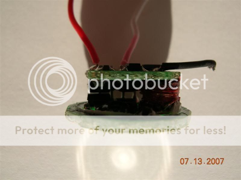
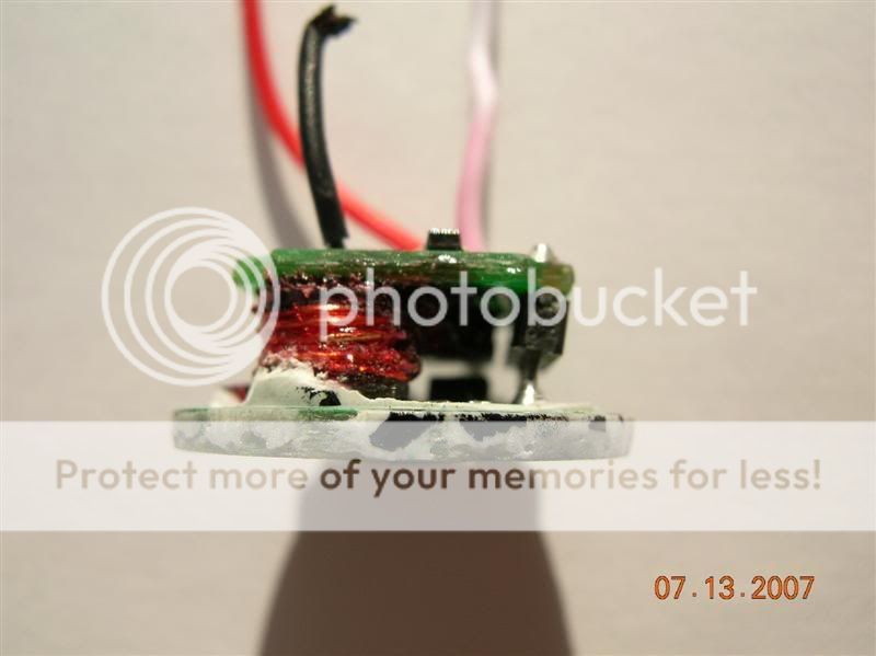
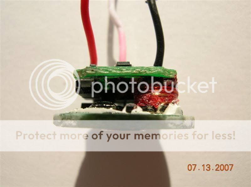
Ask and you shall receive. I know they are crappy though...that's why I didn't post them at first, my SLR is trashed (2 year old got a hold of it), and this little digital camera doesn't take the best shots.

DSCN4090Medium.jpg


DSCN4092Medium.jpg


DSCN4093Medium.jpg


DSCN4094Medium.jpg

That little black goop on the chip in the front is the microcontroller I believe. All you can see from this angle is a shiny black dome.


It was really hard to get any shots of the side. As far as desoldering it all to see inside - after I send the unit to RV7 to test the modes - maybe I'll do that...but for now, I think everyone wants to know actual efficiency numbers out of this board. :naughty:
 
Last edited:
Re: Fenix LxD/P2D boost driver revealed. More pics inside!! Theories of operation wan

Salute. :twothumbs

cant wait for real numbers :)
 
Re: Fenix LxD/P2D boost driver revealed. More pics inside!! Theories of operation wan

Ask and you shall receive. I know they are crappy though...

It was really hard to get any shots of the side.

Wow. Not that crappy. Good stuff. An improvised light tent might help light up the dark corners inside. (pillowcase and floodlighting ?).
 
Re: Fenix LxD/P2D boost driver revealed. More pics inside!! Theories of operation wan

Nice job and nice pics Wintermute :twothumbs

Do you plan to dump the contents of the microcontroller?
 
Re: Fenix LxD/P2D boost driver revealed. More pics inside!! Theories of operation wan

Great Pics, well done
 
Re: Fenix LxD/P2D boost driver revealed. More pics inside!! Theories of operation wan

More side pictures - I used a soldering rig with a magnifying lens and a Fenix L1D to illuminate into the middle of the driver:

DSCN4185Medium.jpg


DSCN4181Medium.jpg


DSCN4169Medium.jpg


DSCN4175Medium.jpg


DSCN4173Medium.jpg


DSCN4182Medium.jpg


DSCN4160Medium.jpg


DSCN4193Medium.jpg


Planning to send this thing off today to RV7 for some testing. In these pics you can really see that microprocessor covered with a layer of black goo. Also, if you look close, there seems to be another coil behind the main large one. Can anyone come up with any more ideas on this thing??

Take care. :wave:
 
Last edited:
Top