Luminus SBT-70 Announced

saabluster

Flashlight Enthusiast
Joined
Oct 31, 2006
Messages
3,736
Location
Garland Tx
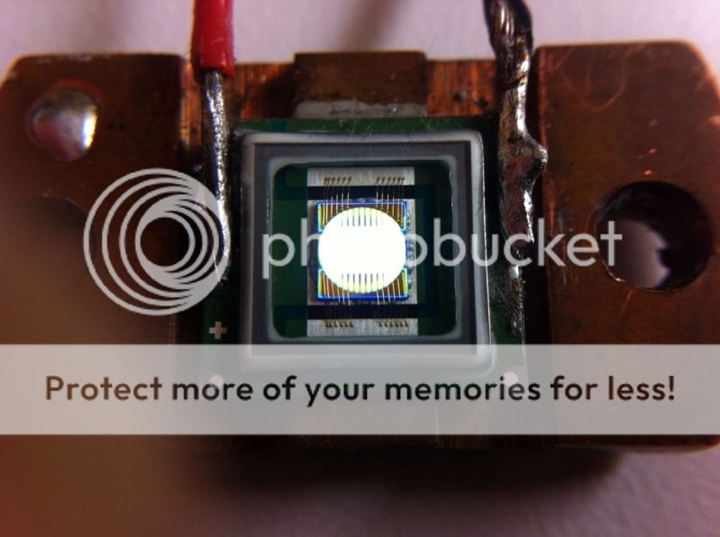
I can see how the circular LED could end up with a lot of waste UNLESS the dies are cut from a rod instead of from a wafer. However, if a wafer is used, a hexagonal die would have comparable optical properties to a circular die, but with zero wasted wafer area.

They would never do that. More cost effective to use large wafers and remove the unwanted portion than to create tiny wafers that would need all new machines to process and then have tiny yields. In fact that is a crazy bad idea. No offense meant. The hexagonal idea? Well sure you could do that. But I believe the processes to do that are covered by patents from another company and wouldn't necessarily be as good optically for certain applications.

CBT-140 don't have white, only RGB - unless I'm missing something?

You are thinking of the CBT-40. I said CBT-140. Very different animal. The CBT-140 is to my knowledge the largest monolithic die yet capable of drive current over 27A! Think of it as a grown-up version of the SBT-70.
 

saabluster

Flashlight Enthusiast
Joined
Oct 31, 2006
Messages
3,736
Location
Garland Tx
Oooops learn to read glenn! ;0)

So are you going to make me a DEFT CBT-140 huh! can you huh? :D
We shall see.

c493b3be.jpg


This next image is processed slightly to enhance contrast.
38858647.jpg


You can clearly see that the active region extends to the corners of the device. Unclear in this is whether or not the area under the gold layer is active as well. If so that seems like a massive waste of power unless there is some waveguiding and subsequent escape of the light into the phosphor.
 

fyrstormer

Banned
Joined
Jul 24, 2009
Messages
6,617
Location
Maryland, Near DC, USA
They would never do that. More cost effective to use large wafers and remove the unwanted portion than to create tiny wafers that would need all new machines to process and then have tiny yields. In fact that is a crazy bad idea. No offense meant.
No offense taken. It is doable, however, which means that eventually someone will do it. In fact someone may already be doing it. There may well be applications where the benefits of true round dies cut from thin rods are worth the associated costs. If not now, then it might still happen eventually, as current die-manufacturing technology is borrowed from microprocessor foundries where the funky optical properties of a square die in a round reflector are completely irrelevant.
 

bshanahan14rulz

Flashlight Enthusiast
Joined
Jan 29, 2009
Messages
2,819
Location
Tennessee
I was gonna say shame on you for only posting a teaser image, but then I clicked on over to page 3. Very very interesting! I think somehow they nil'd the active layer. I can't imagine it being a very good idea to just slather some gold on top to block out all but a circle...
 

SemiMan

Banned
Joined
Jan 13, 2005
Messages
3,899
No offense taken. It is doable, however, which means that eventually someone will do it. In fact someone may already be doing it. There may well be applications where the benefits of true round dies cut from thin rods are worth the associated costs. If not now, then it might still happen eventually, as current die-manufacturing technology is borrowed from microprocessor foundries where the funky optical properties of a square die in a round reflector are completely irrelevant.

- well other than the fact you are normally processing hundreds if not thousands of die at once to reduce cost
- if you ignore thermal issues near the edges of the die
- etc.

Just because something can be done, does not mean it will be done. I won't say never though.
 

blasterman

Flashlight Enthusiast
Joined
Jul 17, 2008
Messages
1,802
There may well be applications where the benefits of true round dies cut from thin rods are worth the associated costs.
See the applications at the beginning of this thread where current square dies are being used.
 

fyrstormer

Banned
Joined
Jul 24, 2009
Messages
6,617
Location
Maryland, Near DC, USA
The replies to my post suggest a lack of basic reading comprehension. I never said there wouldn't be unique engineering and manufacturing constraints with round-die emitters, or that the cost wouldn't be higher. I said there may be applications where the benefits are worth dealing with those unique constraints and additional costs.
 

saabluster

Flashlight Enthusiast
Joined
Oct 31, 2006
Messages
3,736
Location
Garland Tx
The replies to my post suggest a lack of basic reading comprehension. I never said there wouldn't be unique engineering and manufacturing constraints with round-die emitters, or that the cost wouldn't be higher. I said there may be applications where the benefits are worth dealing with those unique constraints and additional costs.

Well I could say the same fyrstormer. It is clear to me you do not understand the significance of what I wrote or the LED making business. Yes it can be done but the astronomical cost means it simply will not be done. I am not one prone to making very absolute comments around here so maybe my "never" comment was a bit too extreme. So instead I will say it is very very very unlikely regardless of the application*. Seriously. What exotic application can you think of that could provide enough volume to prevent the end product from being thousands of dollars per device? How would said device be better than a simple ablation of unwanted die area resulting in an equally round active area?


*I say this with one caveat. I can see some university lab doing something like this just to see what's possible but that's it about it.
 

IMSabbel

Enlightened
Joined
Dec 4, 2004
Messages
921
I am not as hesitating as saabluster.
This is one of the very very view areas that I will definitively say: It will NEVER happen.

Seriously, the idea of using a thing rod (<1cm) for making cicular leds is ridiculous on several levels.

1. Each led size would require a whole substrate handling toolchain. Something like that can cost dozends of millions. (Not to mention that handling tiny weeny wavers would suck in general)
2. Serialization of fabrication: Each step would need to be done for each led indiviudally, instead of 100s of leds in one go.

1+2 would mean that the fabrication would be extremely expensive (even in mass production environment, 100s of $ per device. The idea of it being cheaper than losing 20-30% of the substrate area due to cutting away is ludicrious.

But thats not really the KO-criterium. What is is:

3. THere is a reason you never use the outermost regions of substrates. Any bulbs being grown drop in quality to the edges. Making very thin rods would only increase the issues with the crystal quality. The whole idea of "not needing to mill it into a round shape" depends on using the whole substrate up to the outermost um, which will certainly end up in failure (as edge effects will also not help with any of the more esoteric steps of fabrication). To even in the best case, you would need to trip the outermost edges anyway - which totally kills the whole "no milling/cutting" concept.

Any led made that way would certainly have MUCH worse performance characteristics than a normally created one, so even in a university setting I could only imagine it as a proof of non-viability
 

RCantor

Enlightened
Joined
Mar 11, 2011
Messages
593
Location
KC, MO
OK but getting back to the SBT-70 :)

Anyone know how its surface brightness compares to the XR-E and how many lumens per watt and what the Vf is (approximately) and have a Lm @ whatever amp and over driving graph? Or a link? Thanks!
 

Blitzwing

Enlightened
Joined
Apr 15, 2009
Messages
415
Location
Straya
They don't seem to have appeared in many flashlights yet - correct?

I'd love to see one in the likes of the Crelant 7G5, Solarforce Pro-1 etc and driven hard from a pair of 18650's.
 

IMSabbel

Enlightened
Joined
Dec 4, 2004
Messages
921
We shall see.


38858647.jpg


You can clearly see that the active region extends to the corners of the device. Unclear in this is whether or not the area under the gold layer is active as well. If so that seems like a massive waste of power unless there is some waveguiding and subsequent escape of the light into the phosphor.

Hm. Looking at that picture I wonder... It really does not look as if the active region extends to the edge. The blue glow just seems to be too weak.

Is it possible that what you see at the edges is just an effect light going sideways through passive substrate and just coupling out at the edges?
 

Epsilon

Enlightened
Joined
Sep 19, 2010
Messages
463
Location
Netherlands
And they show up in the stores :)

The SBT version first. Maybe the cbt version will come in the near future ;).

Avnet (hope this works, but it's worth the try):
https://avnetexpress.avnet.com/stor...m=sbt70&N=0&Ne=100000&action=products&x=0&y=0
No stock and data yet

Mouser (this will probably work):
http://www2.mouser.com/Search/Refine.aspx?Keyword=sbt70
stock and prices.

Datasheet:
http://www.mouser.com/catalog/specsheets/PDS-002014_Rev 0X_SBT-70 Production Specification.pdf
up to ~1650lumen for cool white
up to ~1350lumen for 90CRI
up to ~ 900lumen for 95CRI
 

Gunner12

Flashaholic
Joined
Dec 18, 2006
Messages
10,063
Location
Bay Area, CA
Hum, efficiency doesn't seem too amazing at 10 A, ~40 lumen per watt max. Surface brightness seems to be ~240 lumen per mm assuming the best of the best (top bin 70 CRI cool white). There is no dome to decrease the apparent surface brightness though, so that's a plus for throw.

The 90 CRI at higher color temperatures does look nice.
 
Last edited:
Top