georges80
Flashlight Enthusiast
Finally got some time to finish assembling the protoype h6flex driver now that the h6cc is shipping and in use.
I figure as something different I'll document some of the steps involved in taking a design into production. Will (wquiles) suggested some folk may get a better appreciation of what goes into a driver design.
Given I've just started on the h6flex, it seems like an opportune time to take pictures and document some of the steps.
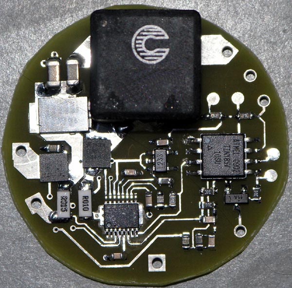
So, here's a picture of a prototype assembled and ready for programming and initial testing:

The prototypes are made as production boards, but to save cost and allow for quick turn and also to allow running several 'flavours' of design and other boards, they have no soldermask/silkscreen and they are also on uncut panels. One key advantage of the bare boards is the ease of making any cuts/jumps and the ease of probing any traces since there is no insulating solder mask in place.
Not having a soldermask makes soldering a little more tricky since not having the mask causes the solder to bridge more easily. But, with good quality flux (I use an RMA flux that is water soluble and washable in a $40 ultrasonic cleaner). With experience I can easily solder fine pitch IC's like the switcher IC on the board.
Once all soldered down it's a case of buzzing out key 'suspect' connections to make sure everything is good enough for power to be applied. I use a current limited supply and slowly raise voltage up from zero to ensure no shorts or high current draw.
The next step is to modify the source code from the other *flex boards and prepare to program it into the prototype board.

The programming & test jig for the h6flex. When laying out the h6flex prototype PCB I also layed out a programming & test jig. The programming part has a 6 pin ISP header to go to an Atmel Dragon (programmer/debugger) and pogo pins to mate with the needed 6 connections on the h6flex board. The test part of the jig has pogo pins that mate with the input power/LED output drive, switch inputs and STAT LED connections.

Here's a shot of the test area of my work bench. Two power supplies and a Tek 200MHz digital scope. Just visible in the lower right is a 50MHz Tek current probe interface that connects to the Tek scope. This allows me to view voltage & current on the scope.

After testing various PWM values and charting the resulting output current I have the necessary data to create the various current tables for the ui-uni2 firmware. Typical of all my flex drivers I provide the user several current tables to choose from. Given this driver is capable of up to 6.6A output I will likely provide 6 tables (tentatively):
1400mA
2000mA
2800mA
5000mA
5600mA
6600mA
Here you can see the excel spreadsheet showing PWM versus output current - very nice & linear.

I'll continue to document the process in this thread as testing continues and then the steps to finish up the design for production boards.
Here's a screen grab to show the PCB layout as it stands, with some minor changes already implemented as refinements to the prototype design are discovered.

cheers,
george.
I figure as something different I'll document some of the steps involved in taking a design into production. Will (wquiles) suggested some folk may get a better appreciation of what goes into a driver design.
Given I've just started on the h6flex, it seems like an opportune time to take pictures and document some of the steps.
So, here's a picture of a prototype assembled and ready for programming and initial testing:

The prototypes are made as production boards, but to save cost and allow for quick turn and also to allow running several 'flavours' of design and other boards, they have no soldermask/silkscreen and they are also on uncut panels. One key advantage of the bare boards is the ease of making any cuts/jumps and the ease of probing any traces since there is no insulating solder mask in place.
Not having a soldermask makes soldering a little more tricky since not having the mask causes the solder to bridge more easily. But, with good quality flux (I use an RMA flux that is water soluble and washable in a $40 ultrasonic cleaner). With experience I can easily solder fine pitch IC's like the switcher IC on the board.
Once all soldered down it's a case of buzzing out key 'suspect' connections to make sure everything is good enough for power to be applied. I use a current limited supply and slowly raise voltage up from zero to ensure no shorts or high current draw.
The next step is to modify the source code from the other *flex boards and prepare to program it into the prototype board.

The programming & test jig for the h6flex. When laying out the h6flex prototype PCB I also layed out a programming & test jig. The programming part has a 6 pin ISP header to go to an Atmel Dragon (programmer/debugger) and pogo pins to mate with the needed 6 connections on the h6flex board. The test part of the jig has pogo pins that mate with the input power/LED output drive, switch inputs and STAT LED connections.

Here's a shot of the test area of my work bench. Two power supplies and a Tek 200MHz digital scope. Just visible in the lower right is a 50MHz Tek current probe interface that connects to the Tek scope. This allows me to view voltage & current on the scope.

After testing various PWM values and charting the resulting output current I have the necessary data to create the various current tables for the ui-uni2 firmware. Typical of all my flex drivers I provide the user several current tables to choose from. Given this driver is capable of up to 6.6A output I will likely provide 6 tables (tentatively):
1400mA
2000mA
2800mA
5000mA
5600mA
6600mA
Here you can see the excel spreadsheet showing PWM versus output current - very nice & linear.

I'll continue to document the process in this thread as testing continues and then the steps to finish up the design for production boards.
Here's a screen grab to show the PCB layout as it stands, with some minor changes already implemented as refinements to the prototype design are discovered.

cheers,
george.


