chesterqw said:
maybe there is some super secret formula for a thermal conductive pcb?
Nah, the techniques have been pretty common for the past decade, nothing new to see here. Usually, where the FR-4 is used in the ones ETGTech supplies, you use instead, a thermally conductitive dielectric material, instead of an insulator material.
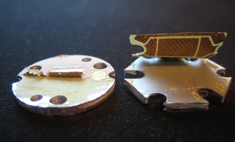
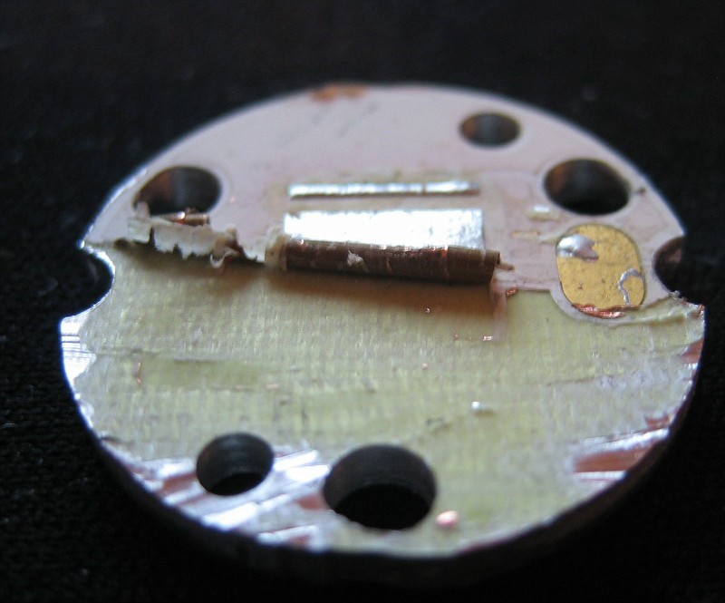
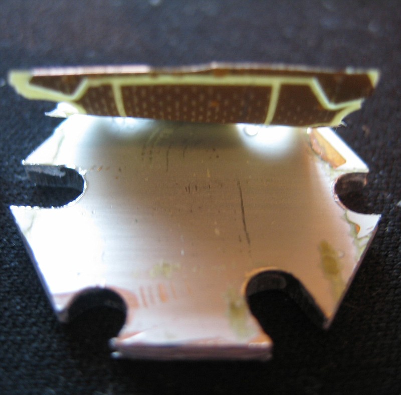
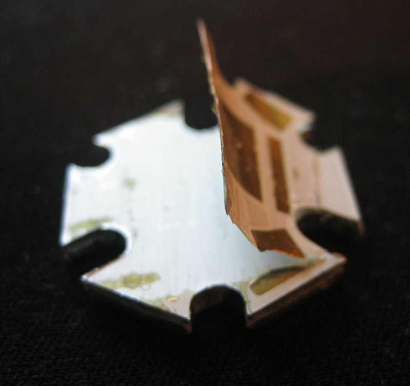
I'm looking at one of these and the FR-4 layer they use looks to be about 12 mils thick, but I do not have one that is unmounted for measurement. If this is in fact correct, the thermal resistance would be about 25 C/W.
Typical MCPCB's from way back when used to use 3 mil thick FR-4, which results in a thermal resistance of about 7 C/W.
Something that came out a few years ago, was a special thermal dielectric material that enhanced the thermal conductivity of the dielectric layer (typically the board material was black in color inside), which has a 3 C/W thermal resistance.
Just simply using 150 vias (which is 100% free in volume manufacturing) under the part can lower the thermal resistance to way below 0.5 C/W. This can be lowered even further by utilizing top and bottom copper layers, flooding from the thermal pad (the copper spot you solder to) across the board surface.
Using vias as thermal transfer points can be quite effective. You could make the board 39 mils thick (1mm), and do nothing more than put only 9 vias of 0.5mm in diameter, and still end up with a thermal resistance of 9 C/W. If you reduce the board thickness to one of the standard pre-preg board materials, like the 3 mil thick material (0.0762 mm), you end up with a thermal resistance of only 0.69 C/W.
Keep in mind, with the CREE, the ceramic material used is not the best for thermal spreading. As such, one would most definitely want to put the vias right under the die area.
So, how does it work in the overall scheme? I took a A19 head with a 2x123 cell body, and with the surface area, very roughly estimate the flashlight has a 30C/W thermal resistance to the ambient air. Using the 12 mil thick FR-4 MCPCB would end up nearly doubling the thermal resistance of the overall solution from the LED die to the ambient air.
However, if one were to carry the flashlight in their hand, as most people do, you always sweat a little, causing a very good thermal path from the hand, to the blood steam, which then pumps the heat away, much like a coolant system does for the engine in a car. Unfortunately, I do not know the exact C/W of this interface, but in this case, the use of the ETGTech MCPCB would be by and far be the highest thermal resistance point, and have a highly significant impact on the overall thermals.
On another note, if you want to go high tech instead:
There have been some developments in the past few years where they use graphite as a thermal spreader (done right, it has a lower spreading thermal resistance than even copper, about 20% better), then use the area advantage to lower thermal transfer thru the board.
An example of one of these newer technologies:
http://www.graftechaet.com/Technical-Documents/Technical-Bullitin/EG-ZS-PP-098.pdf


")

